For decades, the story of computing has largely been written in silicon. Chips became smaller, processors became faster, and machines became capable of handling tasks that once seemed unimaginable. But the demands placed on computing have changed dramatically. AI now requires extraordinary amounts of processing power, memory, bandwidth, and energy, putting increasing pressure on the architecture that has powered the digital age.
That is where light enters the conversation.
Photonic computing offers a different way of thinking about how information can be transmitted and processed. Instead of relying primarily on electrons, it explores the potential of photons to move and work with data at remarkable speeds while addressing some of the energy and heat challenges associated with conventional architectures.
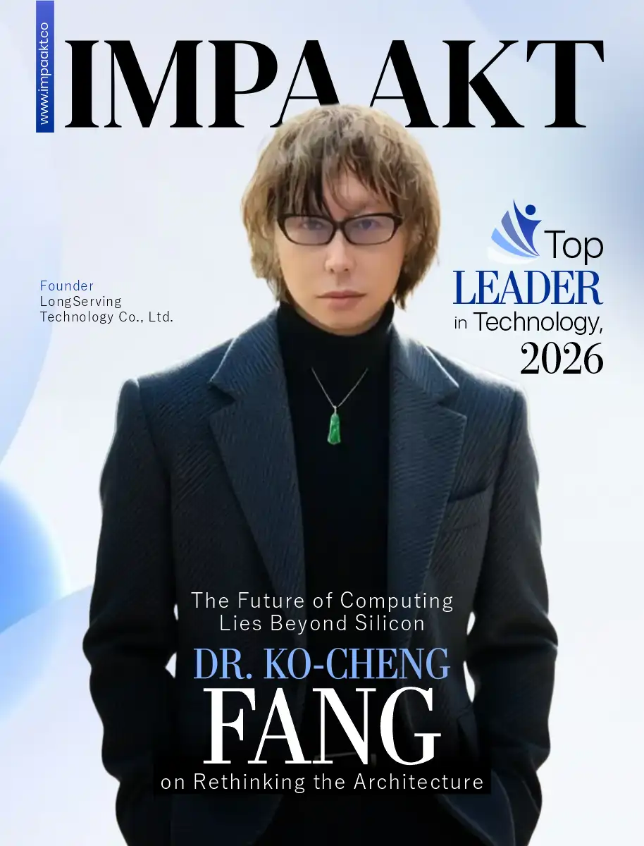
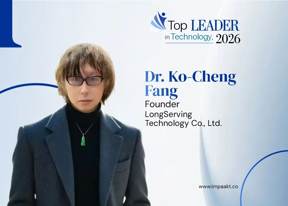
Dr. Ko-Cheng Fang, Founder of LongServing Technology Co., Ltd., has spent years exploring that possibility. His work on X-Photon materials, photonic architectures, and fully optical photonic memory reflects a larger conviction: when an existing technological path begins approaching its limits, the answer may lie in changing the path itself.
What makes his journey particularly distinctive is the range of influences behind it. Science and engineering form the foundation of his research, while art has shaped his sensitivity to structure, space, light, and form. Military history and Zen meditation have further influenced the way he observes patterns and thinks about what lies ahead.
The result is an approach to innovation that rarely stays inside one discipline. Dr. Fang is interested in creating new materials, architectures, and possibilities when existing frameworks appear insufficient. His more than 40 international patents are part of that journey, but his larger ambition is to challenge how people think about what technology can become.
Inspired by the ideas behind his work and his pursuit of a new direction for computing, we got into a conversation with Dr. Fang to explore the science, imagination, and conviction driving his vision of the future.
Dr. Ko, your career brings together science, engineering, entrepreneurship, and even art. Looking back, what experiences shaped your belief that true innovation happens when disciplines intersect rather than operate in isolation?
Looking back on my career and creative journey, I have always believed that true innovation never emerges from within the confines of a single discipline. Instead, it is born from the spark created at the intersection of science, engineering, aesthetics, and intuition.
For me, this interdisciplinary philosophy has been shaped by years of diverse learning and profound personal experiences. My early exploration of painting, sculpture, and other forms of artistic creation cultivated a heightened sensitivity to structure, space, light, and shadow. At the same time, my study of military history and practice of Zen meditation strengthened my ability to think systemically, recognize patterns, and develop an intuitive sense of what may lie ahead.
These seemingly unrelated experiences have enabled me to transcend traditional disciplinary boundaries and integrate materials science, physics, electronic engineering, and artistic aesthetics into a unified approach to innovation. For example, when I undertook the challenge of producing laboratory-grown imperial green jadeite—an achievement widely regarded as impossible—I succeeded by combining advanced deep technology with an uncompromising pursuit of artistic value.
Similarly, in my work on photonic quantum computing, I sought to move beyond the limitations of conventional electronic chips by exploring entirely new approaches to materials and optical architectures. I believe scientific research should never be constrained by the boundaries of established theories. True breakthroughs often arise from the courage to cross those boundaries, challenge conventional assumptions, and pursue what others consider impossible.
This belief continues to shape my work and remains the driving force behind my commitment to interdisciplinary innovation—where science, technology, creativity, and intuition converge to create possibilities that did not previously exist.
Three Forces Behind Dr. Ko’s Innovation
SCIENCE + ENGINEERING + INTUITION
- Science provides the foundation.
- Engineering makes it possible.
- Intuition sees what could come next.
That intersection is where Dr. Ko-Cheng Fang looks for breakthroughs.
Much of your recent work focuses on photonic computing. For readers who aren’t engineers, how would you explain why computing with light could represent such a significant shift in technology?
For readers without an engineering background, conventional electronic chips can be thought of as using “electrons” moving through increasingly narrow pathways. As we push these pathways to operate at ever-higher speeds and densities, heat generation, signal loss, and energy consumption become increasingly difficult challenges.
Photonic computing takes a fundamentally different approach: instead of relying primarily on the movement of electrons, it uses photons—particles of light—to transmit and process information. Because light can carry enormous amounts of data at extremely high speeds while generating far less resistive heat, photonic architectures have the potential to deliver orders-of-magnitude improvements in bandwidth, energy efficiency, and computational throughput for certain workloads.
Today, conventional semiconductor technology is approaching increasingly difficult physical and economic limits. As transistor dimensions approach the 1–2 nanometer regime, phenomena such as quantum tunneling, data-movement bottlenecks, and the enormous challenge of removing heat are making further scaling progressively more difficult. At the same time, the explosive growth of artificial intelligence is driving unprecedented demand for computing capacity, memory bandwidth, and electricity.
Simply continuing to shrink and expand conventional silicon-based electronic chips is therefore becoming an increasingly inefficient path to meeting this demand. Photonic technology offers a fundamentally different route: rather than merely pushing the existing paradigm further, it has the potential to overcome some of its most fundamental limitations and help reshape the infrastructure required for the next generation of AI.
You’ve suggested that conventional semiconductor technology is approaching its physical limits. What opportunities do you believe photonic computing creates that today’s electronic chips cannot?
Conventional electronic chips are facing increasingly severe physical and engineering limits. As semiconductor processes approach the 1–2 nanometer scale, phenomena such as quantum tunneling, the memory wall, and escalating power consumption and heat dissipation have become major obstacles to further scaling. As a result, the traditional trajectory of Moore’s Law is encountering increasingly difficult challenges.
Photonic computing, by contrast, opens up opportunities that conventional electronic architectures cannot readily achieve:
A breakthrough in computing power and speed: By harnessing the high-speed transmission of light and optical computing architectures, photonic systems have the potential to achieve orders-of-magnitude improvements in processing throughput and speed for suitable workloads.
Exceptional energy efficiency: By processing data directly in the optical domain and minimizing repeated optical-to-electrical and electrical-to-optical conversions, photonic architectures can substantially reduce energy consumption and heat generation—an especially important advantage as AI data centers place unprecedented demands on power infrastructure.
Breaking through the memory wall: Through the development of proprietary X-Photon materials and photonic-memory architectures, the goal is to overcome conventional limitations in memory access, data movement, and bandwidth, enabling a fundamentally different approach to high-performance computing.
Every technological revolution begins with someone questioning an accepted assumption. What assumption about computing did you challenge that ultimately shaped your research?
In the field of computing, the greatest assumption I have ever challenged was: “The improvement of computing power must depend on the continued scaling of transistors, and data processing must be built upon conventional electronic architectures and silicon photonics technology.”
For a long time, the industry has firmly believed that continuously reducing the linewidth of copper interconnects and the size of transistors would enable computing power to keep increasing. However, as semiconductor processes move toward the 1–2 nanometer scale, quantum tunneling effects, heat dissipation bottlenecks, and the “memory wall” have already made conventional electronic architectures increasingly difficult to sustain. In addition, the silicon photonics technology commonly pursued by the industry, with wavelengths of approximately 1310–1550 nanometers, is far too large for extremely small circuits, making it fundamentally impossible to achieve true photonic computing at the nanometer scale.
I refused to accept the established framework that “without the right material, there can be no breakthrough.” Since no existing solution was available in the world, I chose to create entirely new elements and architectures: I developed X-Photon materials with an average wavelength of only 2–3 nanometers and further developed fully optical photonic memory. This breakthrough enables data to be processed and stored directly within the optical spectrum without requiring optoelectronic conversion, fundamentally overturning the physical limitations of conventional computing and defining the direction of my research toward the next generation of the photonic AI revolution.
Your work on optical computing spans many years. What has been the most difficult scientific or engineering challenge you’ve had to overcome to move these ideas closer to reality?
In the process of advancing optical computing toward practical applications, the most difficult challenge I faced was “how to overcome the physical properties of light at the nanometer scale, and create the core materials and photonic memory that did not previously exist in the world.”
Traditional silicon photonics technology operates at wavelengths as long as 1,310–1,550 nanometers. Compared with 14-nanometer chip circuitry, this is like “trying to fit a Boeing 747 into a narrow alley”—an apparent impossibility. To overcome this limitation, I started from scratch to create X-Photon materials, which had never appeared in the periodic table of elements, successfully reducing the average wavelength to just 2–3 nanometers.
However, the fundamental nature of light involves scattering and radiation. To control the light, I designed an optoelectronic conversion substrate and a 90-degree vertical refraction technology, successfully locking the scattered light beams onto an extremely fine red line for circuit transmission.
In addition, the industry once questioned that “even with a photonic CPU, if the memory remains electronic, access speed will ultimately still be constrained by electrons.” To completely break through this barrier, I further utilized the characteristics of photons for storing optical energy and invented an array-based “optical capacitance” and logic gates, creating fully optical photonic memory (Photonic Memory). This breakthrough enables data to be stored and processed directly within the optical spectrum, completing the most critical piece of the puzzle for bringing optical computing into practical application.
You hold more than 40 international patents. Do great inventions begin with solving an existing problem, or with imagining possibilities that others haven’t yet considered?
For me, a great invention is never merely an incremental improvement upon existing problems. It begins with imagining possibilities that others have not yet conceived, and ultimately bringing those possibilities into reality to solve fundamental challenges in the real world.
Whether developing cloud-based cybersecurity encryption locks, creating X-Photon materials with an average wavelength of 2–3 nanometers, or challenging conventional assumptions through photonic memory and anti-gravity levitation technology, I have often encountered initial reactions from the outside world that these ideas were extraordinary, even contrary to conventional thinking.
Yet it is precisely because I have the courage to envision future possibilities and transcend the limitations of traditional disciplines that I have been able to create entirely new materials and architectures, addressing fundamental challenges such as the AI energy crisis and computing bottlenecks.
Imagination provides the direction, while rigorous scientific validation transforms possibilities into great inventions that can genuinely improve human life.
As Founder of LongServing Technology, how do you create a culture where ambitious ideas are encouraged while maintaining scientific discipline and commercial focus?
I believe the key to building this kind of culture lies in the deep integration of forward-looking breakthrough thinking, rigorous scientific validation, and a clearly defined path to ommercialization.
When it comes to encouraging ambitious ideas, we break through the frameworks and boundaries of traditional disciplines. I encourage my team not to be constrained by existing physical limits or market conventions, but to have the courage to ask, “Is it really impossible?” and to have the freedom to explore unknown fields.
At the same time, we maintain exceptionally high standards of scientific rigor. Every disruptive concept must undergo substantive data validation, prototype development, and verification by third-party laboratories. We never allow bold ideas to remain mere speculation or become driven by short-term market hype.
Finally, we maintain a strong commercial focus. From the very first day of research and development, our ultimate goal is practical commercialization—not simply publishing academic papers or pursuing personal recognition. From X-Photon materials and photonic memory to optoelectronic conversion architectures and patent portfolios, we systematically develop the commercial infrastructure, manufacturing partnerships, and supporting mechanisms tailored to each technology, ensuring that ambitious innovations can ultimately be transformed into tangible products that improve human life and create sustainable value.
Technology leaders today must balance vision with execution. How do you decide which ideas are worth pursuing and which should remain on the drawing board?
My core criteria are: “Does the technology possess the disruptive value to solve major future bottlenecks, and are the corresponding conditions for commercialization and production already mature?”
For me, an idea worthy of immediate investment must have the potential to fundamentally address a critical problem facing humanity. For example, as AI computing power encounters the “memory wall” and an enormous strain on the power grid, we chose to immediately devote substantial resources to the commercialization and mass-production planning of X-Photon materials and photonic memory, because we believe this is an urgent priority for reshaping the computing architecture of the future.
Conversely, if an idea is highly forward-looking but the current industrial supply chain, equipment, and market acceptance are not yet ready, I will strategically protect it through precise patent positioning while keeping it on the drawing board. For example, my early work in cloud cybersecurity and encryption locks, as well as the anti-gravity levitation technology currently under confidential development, follow this approach. We first complete the core theoretical work and prototype validation, then wait for the convergence of technological maturity and market demand before bringing the technology to the world at the most appropriate moment.
If AI and photonic computing reach the potential you envision, which industries or aspects of everyday life do you believe will experience the greatest transformation first?
If AI and photonic computing achieve the breakthroughs we anticipate, the first area to undergo a profound transformation will be AI infrastructure and cloud computing centers.
Today, conventional electronic chips are facing severe challenges from high energy consumption, heat dissipation limits, and the “memory wall” bottleneck. Photonic computing has the potential to deliver more than 1,000 times greater computing power while reducing energy consumption by more than 90%. This means that a single photonic AI computing center could potentially deliver performance comparable to hundreds of conventional data centers, fundamentally addressing the power and cooling crisis.
The industries that will subsequently experience dramatic transformation include:
Biotechnology, healthcare, and drug discovery: Massive photonic computing power could dramatically shorten the time required for genome sequencing and molecular simulations for new drug development, accelerating the adoption of precision medicine.
Intelligent robotics and autonomous driving: Millisecond-level ultra-low latency combined with powerful computing capabilities could give systems powered by “photonic AI” real-time reasoning capabilities, making highly safe autonomous decision-making a practical reality.
Everyday life and edge devices: When photonic AI is integrated into smartphones and everyday electronic devices, people could have powerful AI assistants running directly at their fingertips, fundamentally changing the way humans interact with technology and communicate with data.
When future generations look back on your work, what do you hope they will remember most: the inventions themselves, the problems they solved, or the way they changed how people think about innovation?
If future generations look back on my work, what I hope they remember most is: “We fundamentally changed the way people think about innovation.”
The inventions themselves—such as X-Photon materials, photonic memory, or laboratory-grown jadeite—will inevitably be surpassed by newer technologies as time progresses. The problems these inventions address, such as AI computing bottlenecks and energy crises, will likewise be replaced by new challenges as civilization continues to evolve.
But a way of thinking that breaks disciplinary boundaries, dares to question established assumptions, and combines the highest standards of science with aesthetics can transcend generations and continue to inspire those who follow.
I hope future generations can see through my journey that when the entire world believes a particular physical limit cannot be overcome, we do not have to blindly compromise within an old framework. Instead, we can choose to create entirely new materials and architectures.
If my work can inspire future explorers to believe that “there are no boundaries between disciplines, and no limits to innovation,” and to have the courage to imagine and realize possibilities that others have not yet conceived, that will be the most valuable legacy I could leave behind.
Looking ahead ten years, what technological breakthrough do you believe the world is still underestimating today?
I believe the world is currently underestimating the fundamental potential of fully optical architectures—including X-Photon nanophotonic materials and photonic memory—to reshape AI computing power and the energy ecosystem, as well as the breakthrough potential of anti-gravity levitation technology in future transportation and materials science.
Today, global technology giants still place enormous faith in conventional silicon-based electronic chips, investing hundreds of billions of dollars in power plants and cooling systems simply to sustain the continued growth of computing capacity. At its core, this is an inefficient race within a sunset industry. The world has broadly underestimated the fact that photonic technology has already overcome the bottlenecks of nanoscale wavelengths and memory access. Fully optical computing can not only deliver more than 1,000 times greater computing power, but also reduce energy consumption by 90%, directly alleviating the power and thermal challenges facing AI data centers worldwide.
At the same time, the public often views “anti-gravity levitation” as a distant myth or science fiction, underestimating the possibilities that materials science may offer for levitating metals. Once realized, this technology could fundamentally transform humanity’s understanding of mobility and space, opening a new era of low-altitude flight over oceans and unrestricted movement across mountains and other terrain.
Over the next decade, these deep technologies—by challenging established physical frameworks—have the potential to reshape human civilization at a pace beyond our current imagination.